
You have not yet added any article to your bookmarks!
Join 10k+ people to get notified about new posts, news and tips.
Do not worry we don't spam!
Post by : Rohit Dhiman
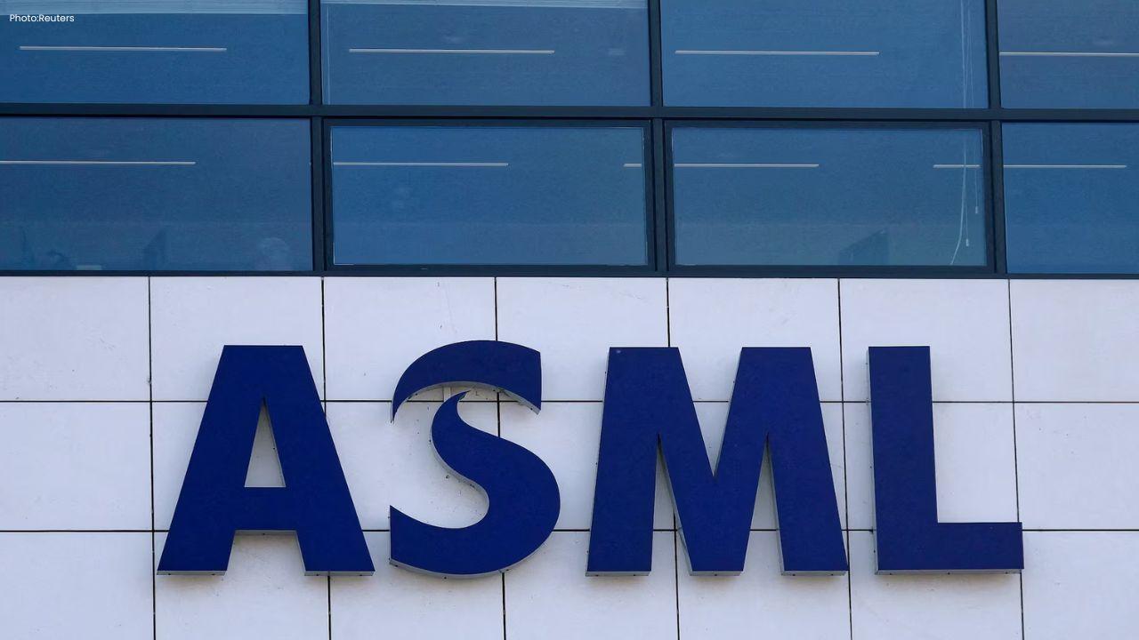
The global semiconductor industry could be approaching another major technological shift, with Dutch equipment manufacturer ASML and German optics specialist Carl Zeiss working on a next-generation chipmaking system that may become available in approximately a decade. The technology, known as Hyper NA, is designed to print even smaller circuit features than those produced by today's most advanced extreme ultraviolet systems. The development could become important for manufacturers seeking to build more powerful, energy-efficient and compact chips for artificial intelligence, data centres, smartphones and other advanced computing applications. However, the technology remains under development, and its eventual commercial availability will depend on overcoming several engineering challenges. According to a peer-reviewed research paper published in the October issue of the Journal of Micro/Nanopatterning, Materials, and Metrology, the proposed system would build on existing technologies rather than require an entirely new manufacturing approach.
Hyper NA is a proposed next-generation lithography system intended to print smaller circuit patterns on semiconductor wafers. It is being developed as a potential successor to ASML's existing High NA extreme ultraviolet lithography equipment. The system is designed to produce features as small as five nanometres, according to the research paper. That would represent a substantial reduction compared with the capabilities described for the current High NA platform. Lithography is a critical stage of semiconductor manufacturing. During this process, specialised equipment transfers intricate circuit patterns onto silicon wafers. The precision of those patterns influences how densely transistors and other components can be arranged on a chip. As manufacturers continue developing advanced processors, the ability to print increasingly fine structures remains important. Smaller circuit features can help support higher transistor density and improvements in performance and power efficiency, although the final benefits also depend on chip architecture, materials and manufacturing techniques.
Demand for advanced semiconductors has increased as artificial intelligence systems, cloud computing services and large data centres require substantial computing capacity. AI processors must handle increasingly complex calculations, while data centre operators are looking for ways to improve performance without allowing energy consumption and operating costs to rise unnecessarily. More advanced semiconductor manufacturing can contribute to these goals by enabling denser circuit designs and improvements in chip performance. However, producing smaller structures also introduces greater demands on manufacturing equipment, optical precision and process control. Extreme ultraviolet lithography uses very short-wavelength light to create extremely fine patterns on silicon wafers. ASML has established a leading position in this specialised equipment market, making developments in its technology particularly significant for semiconductor manufacturers worldwide.
ASML's current High NA equipment represents an advanced generation of extreme ultraviolet lithography systems. The proposed Hyper NA platform would seek to improve patterning capabilities further.
The research paper identifies several important technical points:
Smaller circuit features: Hyper NA is designed to print structures measuring as little as five nanometres.
Existing optical technology: The researchers say Carl Zeiss can already manufacture mirrors with the precision required for the proposed system.
Reuse of existing components: The paper indicates that the current light source could be retained for Hyper NA.
Machine size: The proposed equipment is expected to be only slightly larger than existing High NA machines, which are already exceptionally large.
Further engineering work: Challenges remain before the concept can be turned into a commercially available manufacturing system.
The possibility of reusing existing components could be important because developing entirely new semiconductor manufacturing equipment requires extensive engineering work, specialised facilities and significant investment.
Read Also: Rabada Misses First Australia Test as South Africa Pick Two Spinners
Carl Zeiss is a key optical technology partner in the development of advanced lithography systems. Its expertise in precision optics is particularly relevant because the performance of these machines depends on highly accurate optical components. The Hyper NA research suggests that Zeiss can already produce mirrors precise enough for the proposed technology. That finding provides an important technical foundation, although it does not establish that a complete Hyper NA machine has been built or approved for commercial use. In advanced lithography, even extremely small optical errors can affect the accuracy of the patterns created on silicon wafers. Developing the necessary mirrors and integrating them into a working machine are therefore significant engineering tasks.








ASML and Zeiss Target Next-Generation Chip Technology in 10 Years
ASML and Carl Zeiss are developing Hyper NA technology to print smaller chip circuits, with the next

Rabada Misses First Australia Test as South Africa Pick Two Spinners
Kagiso Rabada misses the opener as South Africa vs Australia begins, with Anrich Nortje returning an

Starc Compares Australia's Tough Year to McIlroy's Major Sweep
Mitchell Starc says Australia winning three away Test series and the World Cup would match Rory McIl

France’s Sesterce Plans $11 Billion AI Data Centre in Finland
Sesterce plans a $11 billion AI data centre in Finland, with major expansion, green energy plans and

Danaher to Launch AI-Powered Autonomous Research Lab in 2027
Danaher plans an AI research lab for 2027, combining robotics and automation to speed up drug discov

Musk Welcomes German Support for Tesla Driver Assistance Tech as EU Approval Push Continues
Elon Musk welcomes Germany's backing for Tesla FSD as the company seeks EU approval amid speed, safe